
Platform Leader: Jacek Jasieniak
Deputy Platform Leader: Udo Bach
Researchers
Solar Industry Partner
International Collaborators
This platform aims to investigate emerging materials within solution-processed solar cell architectures that can go beyond silicon in efficiency or utility. This is being achieved by developing new materials and device architectures through advanced theoretical and synthetic combinatorial screening approaches, advanced device simulation and characterisation methods.
These are being applied to existing solar cell technologies, such as perovskites and copper zinc tin sulphide (CZTS), in order to understand the origin of and, ideally, enhance their efficiencies, as well to a number of novel solar cells materials and device architectures that provide unique advantages compared to traditional silicon-based devices, including those based on back-contact perovskites, semi-transparent and bi-perovskite tandem architectures.
A key aspect of this work package is to harness the advantages of solution-processing for developing high efficiency and low-cost printed solar cells. However, the printing of multi-layered stacks of materials is challenging, particularly when considering the judicious control needed for high-efficiency devices. We focus on understanding the printing processes through insights attained from advanced simulations, that are coupled to ink engineering and printing efforts in order to accelerate the translation of specific materials, such as perovskites, towards larger-scale printing trials and devices at CSIRO.
Materials for Solar Cells: This work package is focused on predicting and synthesising new materials suitable for solar cell applications and their deposition into thin films.
Device Fabrication and Characterisation: This work package aims at setting up a state-of-the-art fabrication and characterisation facility for solution-processed solar cells within the Centre that will enable accelerated development of solar cells. It will also include advanced modelling capabilities that will provide quantitative insights into the operation of emerging solar cells.
Novel Photovoltaic Concepts – Beyond Silicon: This work package will harness new materials and advanced simulation, fabrication and characterisation capabilities to develop novel device architectures for solution-processable solar cells that have the potential to push the efficiency beyond pure silicon or create new utility for photovoltaics.
| Name | Node |
|---|---|
| Jacek Jasieniak | Monash |
| Udo Bach | Monash |
| Salvy Russo | RMIT |
| Asasph Widmer-Cooper | USyd |
| Paul Mulvaney | UoM |
| Timothy Schmidt | UNSW |
| Girish Lakhwani | USyd |
| Ken Ghiggino | UoM |
| Name | Node | Student type |
|---|---|---|
| Qingdong Lin | Monash | PhD |
| Adam Surmiak | Monash | PhD |
| Qianying Guo | Monash | PhD |
| Boer Tan | Monash | PhD |
| Sarah Eskandarian | Monash | PhD |
| Boya Zhao | Monash | PhD |
| Siqi Deng | Monash | PhD |
| Jize Lin | Monash | PhD |
| Jingsong Lin | Monash | PhD |
| Bin Li | Monash | PhD |
| Chun Kiu Ng | Monash | PhD |
| Monika Michalska | Monash | PhD |
| Madhuranga Rathnayake | USyd | PhD |
| Name | Node |
|---|---|
| Sonia Ruiz Raga | Monash |
| Kevin Rietwyk | Monash |
| David McMeekin | Monash |
| Sebastian Fürer | Monash |
| Tian Zhang | Monash |
| Nirmal Peiris | Monash |
| Naresh Chandrasekaran | Monash |
| Juen-Eun Kim | Monash |
| Jae Choul Yu | Monash |
| Stefano Bernardi | USyd |
| Wenxin Mao | Monash |
| Xiongfeng Lin | Monash |
| Dr Tharindu Warnakula | Monash |
| Sri Matta | RMIT |
| Nastaran Meftahi | RMIT |
In this work package we have investigated several material processing approaches and material phenomena within thin film structures suitable for high efficiency perovskite solar cells.
Sequential deposition or two-step processing provides the opportunity for scalable deposition of perovskite materials. We have shown that through a simple solvent engineering approach, the microstructure of the starting lead iodide (PbI2) films can be controlled. This enables the formation of perovskite to be greatly enhanced when exposing the optimised mesoporous lead iodide films to methylammonium halide solutions (Figure 1). Through this approach, among the highest efficiency methyl ammonium lead halide planar devices have been demonstrated.
While the fabrication of perovskites films is critical, the instability of such deposited films is equally important. We have demonstrated that photoinduced halide-ion segregation can be completely reversed at sufficiently high illumination intensities. This has profound ramifications for the use of such perovskites, as it suggests that they should enable more stable devices under high light conditions. The ability to control the local halide-ion composition with light intensity opens opportunities for the use of mixed-halide perovskites in concentrator and tandem solar cells, as well as in high-power light-emissive devices and optical memory applications.
Critical to the formation of achieving low-cost perovskite devices is their ability to be deposited at scale, likely using roll-to-roll (R2R) printing approaching. In R2R printing of solar cells, plastic substrates (typically polyethylene terephthalate, PET) are desirable for their transparency, flexibility and toughness, but are often susceptible to degradation and dimensional distortion at high temperature (greater than 140°C). In collaboration with the Commonwealth Scientific and Industrial Research Organisation (CSIRO) we are working to develop low-temperature charge transport layers suitable for large scale printing. We have developed a microwave-assisted “benzyl alcohol” based nanoparticle synthesis route as an effective one-pot synthesis approach to produce tin oxide (SnO2) nanoparticles (ave. particle size of 5 nanometres) in a single reaction vessel which can be directly used in fabricating SnO2 thin films on plastic substrates at low-temperatures (< 140 °C). This alcohol-based SnO2 ink was successfully used to fabricate electron transport layers (ETL) of planar perovskite solar cells on glass and flexible substrates by spin-coating and R2R coating techniques. A device efficiency over 18% was achieved with SnO2 ETL thermal processed at only 140°C for two minutes. Meanwhile, comparative devices were fabricated using slot-die coated SnO2 ETLs on glass substrates and plastic substrates by R2R printing to yield devices with efficiencies of 15.3% and 10.4%, respectively (Figure 2).
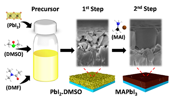
Figure 1. Schematic illustration of the methylammonium lead iodide film formed by the mesoporous lead iodide film.
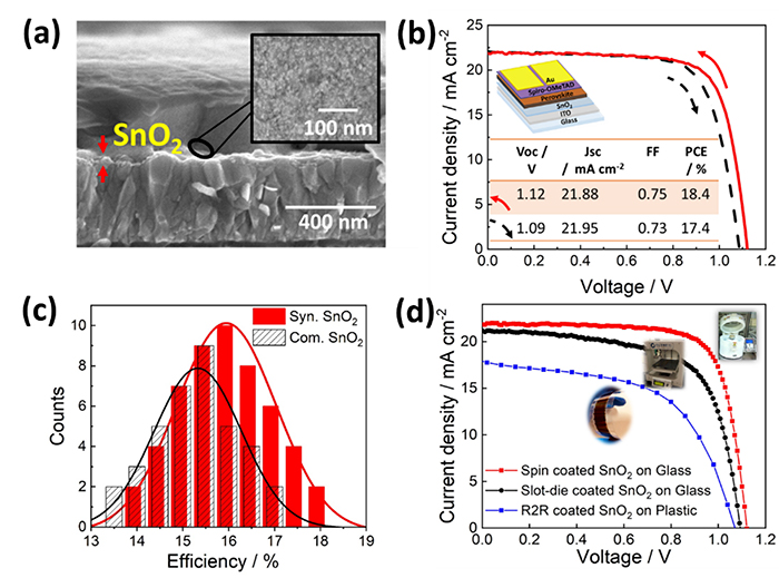
Figure 2. (a) Cross-sectional image of FTO/spin-coated SnO2/perovskite interface (Inset- top-view of SnO2 film on FTO), (b) Current density and voltage characteristics of perovskite solar cell made by spin-coated SnO2 ETL annealed at 140°C for 2 min, (c) PCE distribution of ~50 samples for perovskite solar cells and (d) The best J–V characteristics of the solar cells using spin-coated, slot-die coated and R2R coated SnO2 ETLs annealed at 140°C for 2 min (compared the reverse scans).
Recent developments in hybrid organic−inorganic lead halide perovskite solar cells (PSCs) have shown that use of a two-dimensional (2D) perovskite capping layer on a 3D perovskite absorber layer (3D/2D PSCs) results in substantially improved environmental stability of the devices.
However, in these 3D/2D PSC structures the poor charge-transporting properties through the 2D layer hinder device performance, particularly for thicker 2D layers. Here, we report a facile method that overcomes some of the inherent challenges in using such 2D capping layers that are modified by an additional molecular additive. It is found that this additive provides a passivation effect, which also modifies the crystalline domain sizes of the 2D perovskite. PSCs incorporating this modified 2D capping layer improved charge extraction and reduced charge recombination properties compared with 3D/2D PSCs comprising an unmodified 2D capping layer. This modification results in 3D/2D PSCs for which the maximum power conversion efficiency is increased to more than 20% compared with 18.2% for unmodified 2D capping layers (Figure 3).
In addition to interface engineering, controlling the optical and electrical properties via compositional engineering remains the other key factor for developing high efficiency perovskite devices. Here, we have investigated the microstructural, optical and solar cell characteristics of triple cation mixed anion perovskite solar cells as a function of composition. Our results revealed that optimum compositions provide negligible structural phase impurity, while also coinciding preferential crystal orientation (Figure 4). It was shown that the absence of secondary phase and oriented crystals helps in improving the charge transport inside the device and results in increased solar cell performance. The findings presented here elucidate the microstructure evolution process in different mixed cation perovskites and their role on the charge carrier dynamics and device performance which helps to develop new perovskite materials for high-performance solar cells.
As a final piece of highlighted work, we have expanded our capabilities focused on rapid characterization of solar cells. The presence of damage or imperfections in perovskite solar cells undermine performance and prevent commercial up-scaling. We developed a method for rapid visualisation of macroscopic defects that quantifies the local series resistance and its impact on performance (Figure 5). The next step in this work is to employ our technique to in-line processing for automated process control and validation of perovskite solar cells during manufacturing.
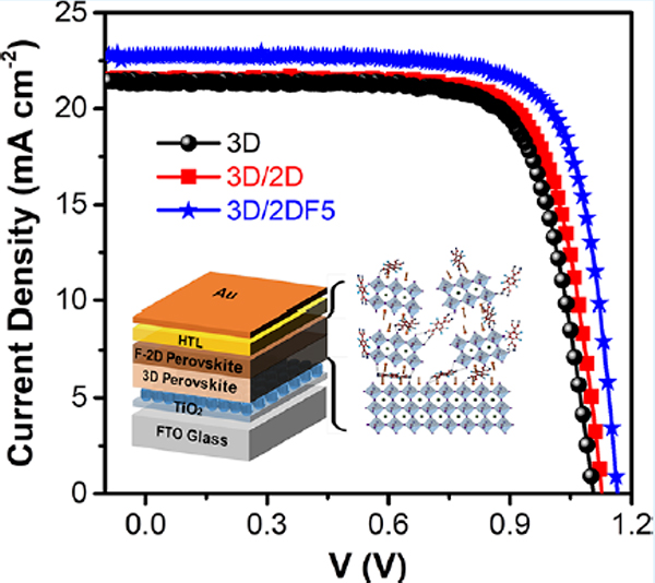
Figure 3. The change in J-V characteristics of perovskite solar cells with and without 2D capping layer.
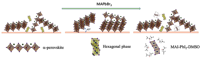
Figure 4. Schematic representation of microstructure evolution with increase (left to right) in the concentration of MAPbBr3 in Cs-FA0.9-x MAx mixed perovskite films.
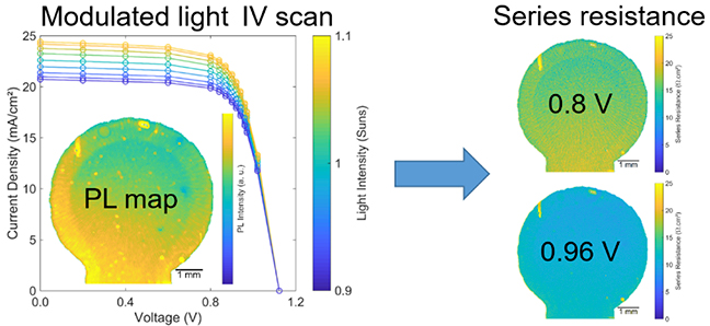
Figure 5. Maps of the voltage dependent series resistance of a perovskite solar cell determined from light modulated IV scans camera-based luminescence.
In this work package we have worked on several novel photovoltaic concepts.
One of these has been the work on high-performance and stable semi-transparent perovskite solar cells (ST-PeSCs). Such devices permit solar cells to operate as electricity-generating windows. This work has looked at device engineering of the solar cell to achieve very high stability while maximizing the efficiency of the devices. In particular, we explored the use of a solution-processed cross-linked hole-transport layer (HTL) formed from VNPB molecules as an alternative to the conventional Spiro-OMeTAD within a conventional semi-transparent perovskite device architecture. Through an optimized multi-step thermal treatment process that maximized charge extraction and reduced recombination from these devices, we could achieve semi-transparent perovskite solar cells that exhibited record power conversion efficiencies for Spiro-OMeTAD-free devices with average visible transmittance values between 10 and 30% (Figure 6).
The other novel concept that we have been developing is based on perovskite tandem solar cells. Such technologies provide a major opportunity for developing photovoltaic devices that can go beyond their fundamental limits, as defined by the Shockley-Queisser limit. One of the biggest challenges for such devices is the need to improve the operational stability of perovskite devices under accelerated aging conditions. In collaboration with the group of Professor Henry Snaith from Oxford we have been working to precisely control the crystallisation process of metal halide perovskites using crystallisation additives to achieve larger grain sizes, higher texture and crystallinity (Figure 7). These improvements in crystallinity resulted in higher thermal, light and moisture stability. A long-term operational encapsulated device stability of T80 = 1410h under full spectrum at 65°C has been achieved. The next steps will require quantifying the stability improvements for solution-processed perovskite/perovskite tandem solar cell in a systematic manner.
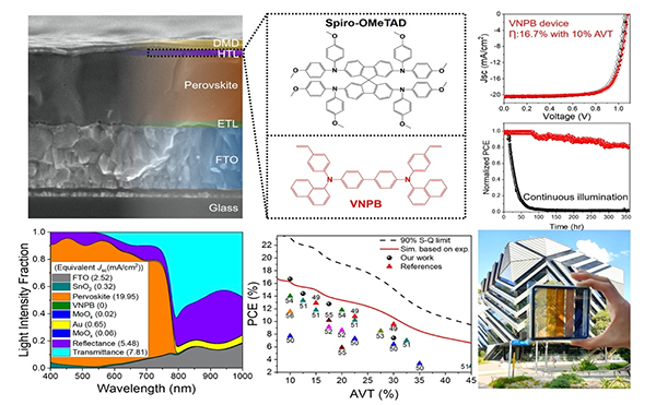
Figure 6. Cross sectional SEM image, chemical structure, J-V characteristics and long-term stability of semi-transparent perovskite solar cells with spiro-OMeTAD and VNPB as hole transport layers (HTLs). Optical simulation, comparison of device efficiency and device picture of semi-transparent perovskite solar cell with VNPB as HTLs..
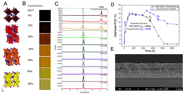
Figure 7. A) Crystal structure of a unit cell during the lead halide perovskite formation. (B) A series of photographs of thin films spin-coated with various amounts of crystallization additive. (C) A series of X-Ray diffraction patterns of corresponding thin film after nucleation process. (D) Champion stability devices under 65°C full spectrum condition. (E) Scanning Electron Microscopy (SEM) cross-section of a solution-processed tandem solar cell.

RayGen is a hybrid energy systems developer located in Australia. We are working with them on understanding failure mechanisms in tandem solar cell modules, with a view to formalising our relationship through an Industry Partnership in the medium term.
Nanjing University
Wuhan University – Perovskite solar cells
Chongqing Institute of Green Technology – As part of the Australia-China Science and Research Fund program on graphene materials.
Activity in NIR materials and solar cells to date continues to be limited.
This has been exacerbated by COVID-19, which has further provided major delays on student and postdoctoral fellow arrivals due to travel and visa issues. These issues may continue into the foreseeable future and are contingent on government policy. Attracting local students and postdocs on such projects is problematic, but needs to be part of a campaign to ensure timely hiring.
Key infrastructure that will enable accelerated materials discovery is set to arrive in 2021, but may take one to two years to be fully commissioned and become operational. Additional resource allocation will need to be requested for us to take full advantage of these new capabilities. There is a risk that operationalising this equipment will reduce productivity across the platform in the interim.
One of the key goals of this platform is to connect the material screening capabilities being developed by CI Russo with appropriate modelling and synthesis.
In November 2020 a cross-node post doc was appointed between Monash and RMIT to develop strong solar cell modelling capabilities within the Centre such that we can correlate experimental and modelling results to genuinely probe the nature of the underlying processes. This is critical to developing the highest efficiency devices, particularly when starting with new materials where so many factors can govern the underlying efficiency. This research project will look to develop 1D, 2D and 3D simulation capabilities that allow microstructure, cavity and scattering effects to be natively introduced. This activity should provide deeper insights into why experimentally developed devices operate with given density-voltage (J-V) and temporal characteristics, and how best to optimise their performance.
Such modelling will complement the developing spectroscopic and device characterisation tools that have been developed or are currently being developed in the Centre. As an example, this year we used ultra-fast measurements (Schmidt lab) to provide insights into carrier dynamics within mixed cation perovskites, while also harnessing micro-second to milli-second photocurrent transients to study the slower recombination processes. The underlying connection between these timescales and their impact on the final device performance was not correlated. Over the next year we hope to introduce modelling into most of our solar cell device work to improve the quality of the work by providing deeper insights into operation of the devices. Moreover, we are also developing several capabilities to further probe the material properties. This includes the assortment of functions on the automated robotic system being current developed by Bach, such as TRPL, transient THz and electrochemical measurements. We are also developing photoluminescence quantum yield measurement capabilities to probe the relative quality of different absorber materials and their interaction with different charge transport layers. This type of measurement will enable for the voltage loss arising from bulk or interfacial defects to be understood, with an aim to optimise the composition and interfacial properties, respectively, as to minimise these effects.
One of the major challenges that we have experienced in the Centre over the past few years is reproducibility in perovskite device synthesis. Many of these devices are fabricated in shared user labs, which lends itself to such outcomes. In the coming year a greater focus on device production reliability will be made. This will be enabled through the successful bid in obtaining a state-of-the-art processing glovebox system that will include deposition and thermal annealing under controlled environments. Moreover, we will be able to correlate the underlying structural evolution of materials and device performance to the condition of the glovebox with dedicated gas sensors. Through this system and controlled fabrication approach, we aim to increase our benchmark perovskite devices from approximately 21% to 22%, as well as increase the obtained stability from 1000 hours to greater than 2000 hours.
These processing control advances will natively facilitate improvements across the various device architectures that we are currently focusing on. Metal halide perovskite will continue to be a major focus.
Efforts within perovskite solar windows will continue with an increased attention given to compositional engineering and module design. Record efficiencies have been demonstrated and stabilities of greater than 1000 hours can now be achieved. However, the current device sizes of approximately 0.1 cm2 is insufficient to demonstrate the technology appropriately and the stability needs to be greater than 30,000 hours to be integrated into any building. A refocusing of activities to overcome these key challenges will be made.
Our collaborative efforts with CSIRO on printed perovskite solar cells have already demonstrated record efficiencies for all-printed devices of greater than 10%. One of the key challenges in these materials is ensuring reliable charge transport layer that can be processed at low temperatures of less than 140°C. Our work on n-type charge transport layers has seen novel aqueous and non-aqueous SnO2 formulations being incorporated within fully printed devices that enabled these record devices to be achieved. The key next challenge will be to demonstrate high efficiency and stability p-type materials. Current work is being placed into NiO nanoparticle systems. This has yielded efficiencies of greater than 18% for small-scale champion devices, but their scalability and implementation into fully printed devices is lacking. This translation will be a key focus of 2021.
Beyond these two device types, we will continue our efforts on perovskite tandems and back-contact solar cells. In collaborations with Snaith’s group from Oxford, we will continue to work on perovskite tandem solar cells. The recent work on crystallisation enhancement using additives will be further developed to show high efficiency and stability perovskite tandems. This work will naturally be adopted within back-contact devices, where a need for high diffusion lengths is a pre-requisite to achieving high efficiency devices. Current back-contact devices are at an efficiency of greater than 6%, but gradual progress around soft-lithographic patterning and compositional engineering will see these efficiencies further progress in 2021.
As a final note, whilst funding has been obtained and the tender processes are currently under way for the automated synthesis and combinatorial sputtering tools, commissioning these tools will require significant time investment in 2021. It is anticipated the preliminary results across these tools will start to emerge in late 2021 or in 2022. New students and postdocs will need to be dedicated to such activities at this period. This will represent a major shift of current activities, particularly from the leading Monash node of this platform.